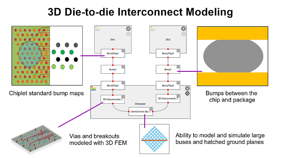

- Keysight Technologies has introduced a new electronic design automation (EDA) tool, 3D Interconnect Designer, aimed at addressing the increasing complexity of interconnect design in chiplet-based and 3D integrated circuit (3DIC) packages.
The solution targets design challenges associated with advanced packaging used in applications such as artificial intelligence infrastructure and data centers. As chiplet architectures become more widely adopted, engineers must manage increasingly complex three-dimensional interconnects in multi-die and stacked-die configurations. Conventional design workflows often require extensive manual intervention to optimize structures such as vias, transmission lines, solder balls, and micro-bumps, while maintaining signal and power integrity in dense layouts.
This manual effort can lead to multiple design iterations and extended development cycles, contributing to higher costs and delayed product introduction. The 3D Interconnect Designer aims to mitigate these issues by automating key aspects of the workflow and enabling earlier validation of design choices.
The tool supports the modeling of complex geometries, including patterned ground planes such as hatched or waffled structures, which are often required to meet manufacturing constraints in silicon-based processes like interposers and bridges. It provides electromagnetic-based simulation capabilities to analyze the electrical behavior of interconnects at both the package and printed circuit board (PCB) levels.
Among its functions, the software enables validation against emerging interconnect standards, including UCIe (Universal Chiplet Interconnect Express) and BoW (Bunch of Wires), early in the design phase. This approach is intended to reduce the likelihood of late-stage design modifications.
The solution can be used either as a standalone tool or integrated within Keysight’s broader EDA environment. It is also compatible with Chiplet PHY Designer, allowing combined optimization of interconnects and physical layer implementations in chiplet and 3DIC systems.
According to Keysight, the objective is to reduce reliance on manual processes, limit design iterations, and provide earlier insight into potential issues related to signal and power integrity in advanced packaging designs.