
- Keysight Technologies, the University of Glasgow, the National Physical Laboratory (NPL), and MPI have developed a broadband characterization method for semiconductor components that enables continuous measurements—from near-DC up to 250 GHz—in a single sweep.
- The demonstration was performed on Indium Phosphide (InP) HEMT transistors intended for applications in millimeter-wave and sub-terahertz bands.
Characterizing transistors across such wide frequency ranges typically requires combining multiple measurement setups, each with distinct calibration procedures. This approach can complicate result comparison and the compilation of consistent data for component modeling. The methodology developed by the four partners aims to minimize these setup changes by performing on-wafer measurements within a single sequence.
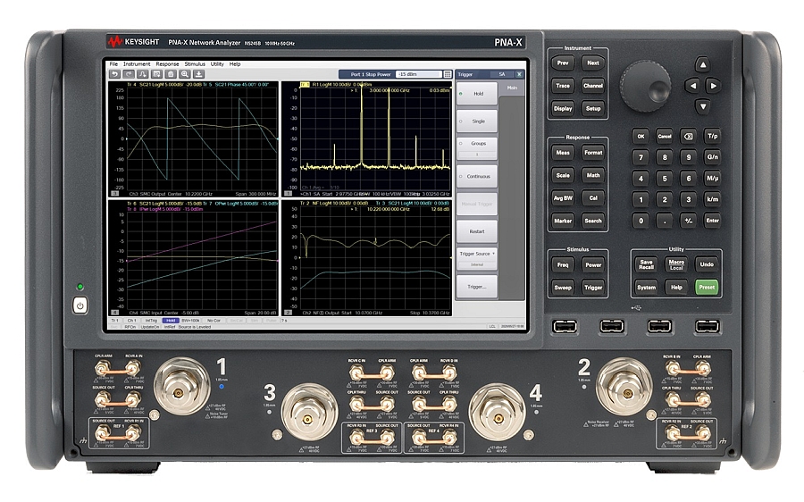
The measurement setup combines a Keysight PNA-X series vector network analyzer (pictured), a frequency extender enabling sweeps up to 250 GHz, and a source/measure unit (SMU). The University of Glasgow provided the InP HEMT transistors and on-wafer calibration standards. MPI integrated its broadband probing technology and calibration software, while the NPL contributed high-frequency metrology and calibration methods.
Avoiding setup or configuration changes
Measurements are performed using a single probe contact, spanning from near-DC to 250 GHz. According to the partners, this setup notably eliminates the need to switch test benches or configurations between different frequency ranges and ensures continuity in S-parameter measurements. The system also incorporates source filtering and calibration functions designed to control the signal applied at the probe tip at millimeter-wave frequencies.
The experiment focuses on InP HEMT transistors, a technology being studied particularly for very-high-frequency applications. The ability to characterize these devices across a continuous range—from low frequencies up to 250 GHz—can provide data for modeling and for studying their behavior as operating frequencies approach the sub-terahertz range.
This collaboration thus integrates measurement instrumentation, on-wafer probing, semiconductor devices, and high-frequency metrology into a unified methodology. The partners state that this approach can be used for research and development on components designed for millimeter-wave and sub-terahertz frequencies.