
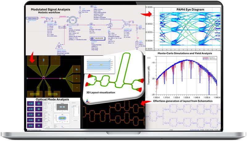
- Keysight Technologies and Win Semiconductors have announced the development of a joint workflow for designing gallium nitride (GaN)-based monolithic microwave integrated circuits (MMICs).
- This solution aims to secure the critical “tapeout” phase by combining multi-domain simulation and physical verification within a unified environment.
In the radio frequency (RF) chip development process, submitting the final design to the foundry—or “tapeout”—is a high-stakes step involving significant time and financial investment. Any undetected design flaw necessitates additional manufacturing cycles, delaying time-to-market by weeks. The implemented workflow automates the simulation, optimization, and verification steps required prior to production.
The unified environment enables multi-domain simulations directly on the chip, manages 3D routing with integrated verification tools, and prepares for the transition to physical testing. This protocol is designed for engineers developing chips for 5G communication infrastructure, Wi-Fi access points, satellite payloads, and radar sensing systems.
Co-design of the Integrated Circuit and Evaluation Board
A key feature of this solution is that it accounts for the component’s overall environment from the initial design stages. MMIC buyers typically make component validation contingent upon results obtained from physical evaluation boards. These boards combine the MMIC chip, its protective package, the printed circuit board (PCB), and RF test connectors.
The workflow enables the co-modeling of these various structural elements. This approach ensures that the performance measured in the laboratory on the complete system aligns with the initial integrated circuit simulations. This comprehensive validation comes as the global market for gallium nitride (GaN) RF devices is expanding, with a projected valuation of $2.77 billion by 2031.
Software Integration and Manufacturing Process
From a technical standpoint, the solution leverages the GaN NP 120P Process Design Kit (PDK) developed by Win Semiconductors. This kit provides the process models and geometric layout rules required for manufacturing.
This foundry data is directly integrated into Keysight’s Advanced Design System (ADS) software suite and RF Circuit Simulation Professional tool. This interoperability enables the implementation of a custom Layout Versus Schematic (LVS) verification solution, formalizing the check between the electrical schematic and the physical circuit layout to validate system compliance prior to the start of industrial production.