
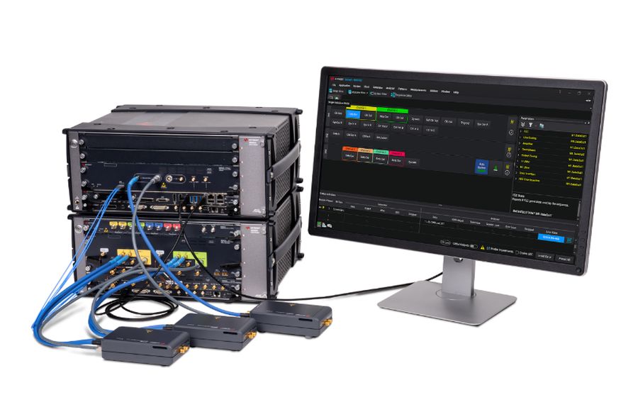
- Keysight Technologies has introduced a protocol test solution for PCI Express (PCIe) 7.0, designed for the validation and debugging of integrated circuits and systems that utilize this interface.
- The solution combines an analyzer, a test generator, a test platform, and analysis software to examine the protocol behavior of links operating at a data transfer rate of 128 GT/s.
- It was showcased at the OCP Global Summit 2026, held from October 13 to 16 in San Jose, California.
The development of this solution comes as computing infrastructure for artificial intelligence increasingly relies on a growing number of interconnections between processors, accelerators, switches, memory, and storage devices. The PCIe 7.0 standard doubles the raw data rate compared to PCIe 6.0, reaching 128 GT/s per lane. This advancement necessitates the verification of link functionality, equipment interoperability, and compliance with protocol specifications.
Analyzing Link Establishment and Data Exchange
Keysight’s solution is designed to analyze the various operational stages of a PCIe 7.0 link, from initial setup to data exchange. Specifically, it provides visibility into the transitions of the Link Training and Status State Machine (LTSSM), which defines the states and steps involved in establishing and managing a link.
The analysis also covers data encoding using Flow Control Units (FLITs)—a mechanism introduced in PCIe 6.0 and retained in PCIe 7.0—as well as protocol errors and transactions occurring at the transaction layer. This information makes it possible to examine exchanges between components and investigate the root cause of observed defects.
Keysight states that its architecture allows for the acquisition of protocol traces without requiring prior configuration of the analyzer. The goal is to reduce the time needed to set up measurements and to facilitate the reproduction of test conditions during debugging phases.
From development to compliance testing
The platform integrates protocol stimulation and analysis functions into a single environment. The test generator allows for the stimulation of equipment under development, while the analyzer provides the data necessary to examine its behavior. The associated software uses the collected traces to identify errors and verify that devices operate in accordance with PCIe specifications.
This approach is designed to cover several stages of development, from initial chip validation to system-level interoperability and compliance testing. It is specifically aimed at detecting protocol issues during the early design phases, before they necessitate hardware modifications or cause development delays.
The solution also supports rack-scale interconnect architectures, which are used in computing infrastructures for AI. Furthermore, Keysight notes that the solution offers backward compatibility, designed to ease the transition from previous PCIe generations and protect investments in existing test equipment.
Joint validation with Synopsys
Keysight reports that it has validated its test solution using PCIe 7.0 intellectual property (IP) from Synopsys. This collaboration aims to verify the operation of the interface between a PCIe controller implementation and 128 GT/s test equipment, with a particular focus on ensuring interoperability between chips and the systems that incorporate them.
This joint validation represents a step in the preparation of next-generation components and platforms intended for data centers and AI infrastructure. However, it does not exempt manufacturers from conducting the necessary testing on their own designs and system configurations.