
- This Analog Devices’s article describes how to protect integrated circuit analog inputs and outputs against high voltage transients, as described by the standards IEC 61000-4-2, IEC 61000-4-4, and IEC 61000-4-5.
- This information provides system designers with the knowledge required to design protection circuitry for system inputs and outputs while achieving the following benefits: ease of protection design, higher protection circuit performance due to reduced number of discrete components required, reduced values of series resistance in the signal path, ease of TVS selection due to wide TVS design window.
- The objective is also to ensure the system-level protection for the standards IEC 61000-4-2 (16 kV air discharge), IEC 61000-4-2 (8 kV contact discharge), IEC 61000-4-4 (4 kV), IEC 61000-4-5 (4 kV), an AC and persistent DC overvoltage protection up to ±55 V, and power off protection up to ±55 V.
Author : David Forde, Analog Devices
External, high voltage transients that interact with a system’s analog input and output nodes can damage the integrated circuits (ICs) within the system if they are not adequately protected. The analog input and output pins of a modern IC are typically protected against high voltage electrostatic discharge (ESD) transients.
The human body model (HBM), machine model (MM), and charged device model (CDM) are the device-level standards used to measure a device’s ability to withstand ESD events. These tests are designed so that a device can withstand the manufacturing and the PCB assembly process, which usually take place in a controlled environment.
Systems that operate in harsh electromagnetic environments are required to withstand high voltage transients on the input or output nodes—and when moving from device-level standards to system-level standards for high voltage transient robustness, there is a substantial difference in the energy levels transmitted to the pin of an IC. Therefore, ICs that directly interface with these system input/output nodes must also be sufficiently protected to withstand the system-level high voltage transients. Failure to account for this protection early in a system design can lead to inadequate system protection, delayed product release, and reduced system performance. This article describes how to protect sensitive analog input and output nodes from these IEC standard transient levels.
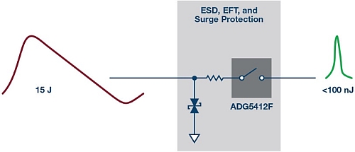
Figure 1. IEC system protection for precision analog inputs.
IEC 61000
IEC 61000 is the standard that covers EMC robustness at the system level. The three sections of the standard that deal with high voltage transients are IEC 61000-4-2, IEC 61000-4-4, and IEC 61000-4-5. These are the system-level standards for electrostatic discharge (ESD), electrical fast transients (EFT), and surge. These standards define the waveforms, test methods, and test levels for evaluating the immunity of electrical and electronic equipment when subjected to these transients.
The primary purpose of the IEC 61000-4-2 test is to determine the immunity of systems to external ESD events outside the system during its operation—for example, if a system input/output comes in contact with a charged human, cable, or tool. IEC 61000-4-2 specifies testing using two coupling methods: contact discharge and air gap discharge.
IEC 61000-4-4 EFT testing involves coupling a number of extremely fast transient impulses onto the signal lines to represent transient disturbances associated with external switching circuits that are capacitively coupled onto the signal lines. This testing reflects switch contact bounce or transients originating from the switching of inductive or capacitive loads, all of which are common in industrial environments.
Surge transients are caused by overvoltages from switching or lightning transients. Switching transients can result from power system switching, load changes in power distribution systems, or various system faults, such as short circuits and arcing faults to the grounding system of the installation. Lightning transients can be a result of high currents and voltages injected into the circuit from nearby lightning strikes.
Transient Voltage Suppressor
Basic parameters of a TVS:
A transient voltage suppressor (TVS) can be used to suppress voltage surges. They are used to clamp high voltage transients and shunt large currents away from sensitive circuitry. The basic parameters for a TVS are:
- Working peak reverse voltage: The voltage below which no significant conduction occurs
- Breakdown voltage: The voltage at which some specified conduction occurs
- Maximum clamping voltage: The maximum voltage across the device when conducting the maximum current specified
There are a number of factors that must be considered when using a TVS device on a system input or output. An ESD or EFT event will generate a very fast time (1 ns to 5 ns) transient waveform, resulting in an initial overshoot voltage on the system input before the TVS device clamps at its breakdown voltage. A surge event has a different transient waveform with a slow rise time
(1.2 µs) and long duration (50 µs) pulse, and in this event the voltage will be initially clamped at the breakdown voltage, but it can continue to increase to the TVS maximum clamping voltage. In addition, the TVS must be higher than any tolerated dc overvoltage that could be caused by miswiring, loss of power, or user errors to protect the system against this dc overvoltage event. All three situations can cause a potentially damaging overvoltage on the input to the downstream circuitry.
Analog Input Protection Circuit
In order to fully protect a system input/output node, the system must be protected against dc overvoltages and high voltage transients. Using a precision, robust overvoltage protection (OVP) switch at the system input combined with the TVS can protect sensitive downstream circuitry (for example, analog-to-digital converters or amplifier inputs/outputs), as it can be used to block overvoltages and suppress residual currents that are not shunted to ground by the TVS.
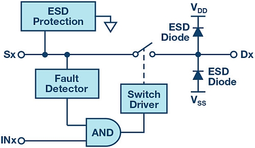
Figure 2. OVP switch functional block diagram.
Figure 2 shows the functional block diagram of a typical overvoltage protection switch; note that this switch does not have ESD protection diodes referenced to its supplies on its input node. It instead has an ESD protection cell that triggers above the devices maximum standoff voltage, which enables the device to stand off and block voltages beyond its supplies. As an analog system typically requires that only the outside facing pins of the switch need IEC protection, the ESD protection diodes are retained on the internal-facing pins (noted as switch output or drain side). These diodes, though being added, benefit by serving as a secondary protection device. During a short duration, a high voltage transient with a fast rise time-like ESD or EFT, the transient voltage is clamped so the voltage will not reach downstream circuits. During a long duration, a high voltage transient with a slow rise time-like surge, the output voltage of the switch is clamped by the internal protection diodes before the overvoltage protection of the switch is activated and the switch opens to fully isolate the fault from the downstream circuitry.
Figure 3 shows the regions of operation for a system input that interfaces with the outside world. The leftmost region (in green) represents normal operation, where the input voltage is between the supply voltage ranges. The second region from the left
(in blue) represents the range of possible persistent dc or long duration ac overvoltages presented to the input due to loss of power, miswiring, or short circuits. Also included in the diagram, on the far right hand side (in purple), is the trigger voltage for the internal ESD protection diodes of the overvoltage switch. The TVS breakdown voltage (in orange) must be selected to be less than the maximum standoff voltage of the overvoltage protection switch and also greater than any know possible persistent dc or long duration ac overvoltage, in order to avoid inadvertently triggering the TVS.
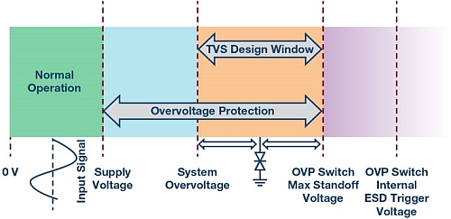
Figure 3. System operation regions.
The following protection circuit in Figure 4 can withstand up to 8 kV IEC ESD (contact discharge), 16 kV IEC ESD (air discharge),
4 kV EFT, and 4 kV surge. The ADG5412F (±55 V overvoltage protection and detection, quad SPST switch from Analog Devices) can withstand the overvoltages caused by ESD, EFT, and surge transients, while the overvoltage protection combined with the protection diodes on the drain protects and isolates downstream circuitry. Table 1 shows the levels of high voltage transients the ADG5412F can withstand various combinations of TVS breakdown voltages and resistors.
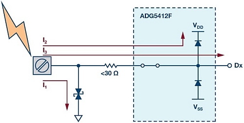
Figure 4. Protection circuit.
Table 1: Testing Results (IEC Air Was Not Tested with 0 Ω Resistor on 33 V TVS and 45 V TVS)
| Protection |
Protection IEC 61000-4-2 ESD Contact Discharge |
IEC 61000-4-2 ESD Contact Discharge IEC 61000-4-2 ESD Air Discharge |
IEC 61000-4-4 EFT |
IEC 61000-4-4 EFT IEC 61000-4-5 Surge |
|
33 V TVS and 0 Ω resistor |
5 kV |
3 kV |
4 kV |
|
|
33 V TVS and 10 Ω resistor |
8 kV |
16 kV |
4 kV |
4 kV |
|
45 V TVS and 0 Ω resistor |
4 kV |
2 kV |
4 kV |
|
|
45 V TVS and 15 Ω resistor |
8 kV |
16 kV |
4 kV |
4 kV |
|
54 V TVS and 30 Ω resistor |
8 kV |
16 kV |
4 kV |
4 kV |
The protection network consists of a TVS and an optional low value resistor. The resistor is required to achieve the higher levels of ESD and EFT protection, as it prevents the internal ESD protection cell of the overvoltage switch from triggering before the TVS clamps the voltage on the input. Figure 4 also shows the various current paths during a high voltage transient event. The majority of the current is shunted to ground through the TVS device (Path I1). Path I2 shows the current that is dissipated through the internal ESD diodes on the output of the ADG5412F, while the output voltage is clamped to 0.7 V above the supply voltage. Finally, the current in Path I3 is the residual current level that the downstream components must withstand. For more details on this protection circuit, please see the application note AN-1436 from Analog Devices.
IEC ESD Protection
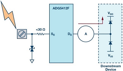
Figure 5. Test circuit.
Figure 6 and Figure 7 show measurements taken during both an 8 kV contact discharge and a 16 kV air discharge IEC ESD event using the test circuit shown in Figure 5. As described previously, there is an initial overvoltage on the source pin before the TVS device clamps the voltage to approximately 54 V. The voltage at the drain of the switch during this overvoltage is clamped at 0.7 V above the supply. The drain current measurement shows the current flowing into the diodes of the downstream device. The peak current of the pulse is approximately 680 mA and the duration of the current is just approximately 60 ns. By comparison, a 1 kV HBM ESD strike that has a peak current of 660 mA has a duration of 500 ns. It is therefore reasonable to conclude that a downstream component with a HBM ESD rating of 1 kV should withstand both an 8 kV contact discharge and a 16 kV air discharge IEC ESD event using this protection circuit.
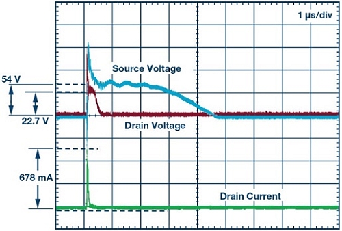
Figure 6. Drain voltage and output current at the drain during an 8 kV event.
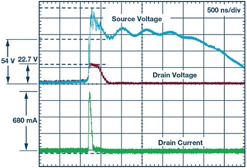
Figure 7. Drain voltage and output current at the drain during a 16 kV air discharge event.
EFT Protection
Figure 8 is a measurement taken during one pulse of a 4 kV EFT event. Similar to what happens during an ESD transient, there is an initial overvoltage on the source pin before the TVS device clamps the voltage to approximately 54 V. The voltage at the drain of the switch during this overvoltage is again clamped at 0.7 V above the supply. The peak current of the pulse flowing into the downstream device in this case is just 420 mA and the duration of the current is just approximately 90 ns. Comparing this again to an HBM ESD event, a 750 kV HBM ESD strike has a peak current of 500 mA and has a duration of 500 ns. The energy is therefore transmitted to the pin of the downstream device during a 4 kV EFT event, which is less than that of a 750 kV HBM ESD event.
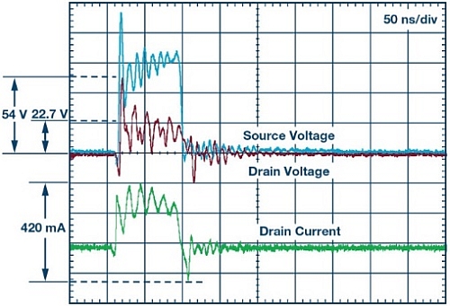
Figure 8. EFT current for a single pulse.
Surge Protection
This measurement in Figure 9 shows the result of a 4 kV surge transient applied to the input of the protection circuit. As mentioned previously, the voltage at the source can increase beyond the breakdown voltage of the TVS up to its maximum clamping voltage. The overvoltage protection switch in this circuit has a reaction time of approximately 500 ns and the voltage on the drain of the device is clamped at 0.7 V above the supply during this first 500 ns time period. The peak current flowing to the downstream device is just 608 mA during this time period and after approximately 500 ns, the switch is seen to turn off and isolate the downstream circuitry from the fault. Again, this is less than the energy transmitted during a 1 kV HBM ESD event.
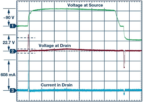
Figure 9. Operation of OVP during a surge event.
Appendix
Analog Devices Overvoltage Protection and Detection Products: ±55 V OVP
|
Part Number |
Configuration |
HBM ESD Level (kV) |
Specifications |
Characterization Voltages (VNOM) |
|||||||||||
|
RON Typ (Ω) |
RON Flatness (Ω) |
On Leakage Typ (nA) |
QINJ Typ (pC) |
BW (MHz) |
Single |
Dual |
|||||||||
|
12 |
36 |
±15 |
±20 |
TSSOP |
LFCSP |
||||||||||
|
ADG5412F/ |
SPST 4 |
5.5 |
10 |
0.6 |
0.3 |
680 |
270 |
EP |
|||||||
|
ADG5412BF/ |
SPST 4 |
3 |
10 |
0.6 |
0.3 |
680 |
270 |
||||||||
|
ADG5436F |
SPDT 2 |
6 |
10 |
0.6 |
0.3 |
654 |
108 |
||||||||
|
ADG5243F |
SPDT 3 |
3.5 |
270 |
7 |
0.3 |
0.8 |
350 |
||||||||
|
ADG5404F |
4:1/mux |
5 |
10 |
0.6 |
0.3 |
680 |
108 |
||||||||
|
ADG5208F/ |
8:1/diff |
3.5 |
250 |
6.5 |
0.3 |
0.4 |
190/ |
||||||||
|
ADG5248F/ |
8:1/diff |
3.5 |
250 |
6.5 |
0.3 |
0.8 |
190/ |
||||||||
|
ADG5462F |
Channel protector |
4 |
10 |
0.6 |
0.3 |
N/A |
318 |
||||||||
About the author :
David Forde joined Analog Devices as a layout engineer in 2006 after graduating from Carlow Institute of Technology with a B.Sc. in integrated circuit design. In 2011, he graduated from the University of Limerick with an M.Eng. in VLSI systems and, in 2015, he joined the Instrumentation and Precision Technology Group as an applications engineer supporting the analog switch and multiplexer product portfolio.