
- While fifth-generation (5G) mobile communication networks are being deployed, research for the development of sixth-generation (6G) wireless technologies is already underway.
- The components used for 6G communication will operate at even higher frequency bands than those used for 5G.
- This poses new testing challenges for characterizing the components used by future 6G communication equipment.
By Navneet Kataria, Product Manager at Anritsu Corporation
1. How do 6G components and materials differ from their 5G equivalents?
Navneet: 6G technology is going to be substantially different from the 5G world. The main driving part for the differentiations is the usage of extremely high frequencies above 100 GHz, from 140 to 240 GHz which provides extreme bandwidths for carrying several Gigabytes of data. In 5G, the frequencies being used are in the range of 28/39 GHz and given the advancement in material packaging/fabrication and measurements, it is much simpler to fabricate, a measure and make the system very efficient. Since the 6G components have to work on extremely high frequencies, they have to be designed, processed, and packaged accordingly. The same methodologies applicable for 5G may not be valid for 6G. The high frequency signals suffer from severe attenuations and many other challenges when propagating through the 6G components and that is why special materials are being continuously discussed as being utilized for 6G. Materials such as SiGe are being used and pushed in the fabrication process for reducing their thickness to approximately 5 mil/2 mil for efficient component developments and minimum signal loss. Considering all these aspects, it is necessary to ensure high accuracy and reliability at high frequencies in the measurement technology for expressing materials performance.
Apart from the material being used for 6G, the other aspect for 6G is the component characterization. Since the 6G devices work at extremely high frequencies, it is very important to characterize these devices to understand how well they perform at higher frequencies. Since these devices are so small in size, their characterization needs special skills and setup which includes a vector network analyser (VNA), a probe station, probes (with very small pitches of the order of 100 um or 75 um) with high resolution camera and a very skilled professional for doing touchdowns on the water level device along with measurement expertise to judge if the calibrations/measurements are good or not. The device characterization is very important especially for device modellers as they are interested to see the broadband response of their 6G devices and check the harmonic contents of their devices. For making broadband measurements they need a broadband sweeping VNA.
2. What performance characteristics are important and what metrics do they need to achieve?
Navneet: From the perspective of materials and their measurements, the key performance characteristics that need to be measured and validated are the material properties such as dielectric constants, effective permittivity, loss tangents, conductivity etc. The parameters are the same as with any technology materials, but the challenges, that have and will creep up, with 6G materials are the measurement techniques for these parameters. Since the thickness of the materials will be so small and it would be expected to work at extremely high frequencies, extreme care needs to be taken while selecting the measurement method and also while making the measurements. Several research papers have been published suggesting various methods for making material measurements, all having their own pros and cons.
From the device characterization perspective the most important characteristics are the S-parameter measurement, which is a measurement of how good/bad the device is performing. S or scattering parameters are an indication of how much signal is reflected back from the device (S11) and how much signal efficiently passes through the device (S21). Performing S-parameter measurements at such high frequencies (of the order of 140 to 240 GHz) comes with its own challenges because of the size of the device and also the behaviour of the device. Various active and passive components have been tested so far in those frequency ranges by Anritsu with the utmost precision and accuracy.
3. What challenges do developers face in testing these components and materials?
Navneet: Material measurements are always very challenging yet very interesting measurements to make. Developers are always in a state of questioning themselves as to:
• Which measurement method is the right fit for their materials? Resonant methods or non-resonant methods? Free space?
• What is more important, accuracy of the measurement or a broadband measurement itself?
• Which measurement method will give them the fastest and most accurate results?
• What fixtures will be able to hold the very thin material/sheet/ substrate?
• What kind of environment do they need to test their material under test (MUT)?
• After making the measurements, how to confirm of the measurements are correct?
All these questions keep haunting developers and creating self-doubts amongst themselves. Choosing the right measurement technique is the most important challenge that needs to be addressed and spent the most time on. Other important challenges are measurement repeatability of the entire system.
From the perspective of device characterization, device developers and especially device modellers are very interested in the harmonic content ( 3rd harmonic, 5th harmonic) of the device under test and that’s why they always prefer having a broadband sweep measurements (covering from very low frequencies to extremely high frequencies e.g., 70 kHz to 220 GHz) for S-parameters. This way they can easily pick up the problematic areas of their devices and make sure they either make changes in the designs or take any other preventive actions. As mentioned above in the introductory question, the main challenge in making these high frequency device measurements are the repeatability in measurements, stability in the measurements with regard to time/temperature and ensuring the accuracy of the measurements.
4. How do these challenges differ from 5G?
Navneet : The measurement challenges in 6G are a little different and a little more complex in nature than in the 5G. For 5G, since the frequencies are comparatively lower (28/39 GHz) than in comparison with 6G, the complexity in fabrication, measurements and testing are relatively simpler than in 6G. Although the basic questions, whether for making material measurements or device characterization, are still the same, but the process of making these measurements is relatively complex in 6G, as highlighted in answers to the above questions.
The challenges are also dependent upon what measurements that the user is trying to make, for example, a user trying to characterize a broadband power amplifier, would need extremely low power levels to be fed into the amplifier, around -50 dBm etc., which is not an easy power to go to at an extremely high frequency range. However, a customer trying to characterize a waveguide component at 140 GHz, may need higher power.
5. What is the role of Vector Network Analysis in these measurements?
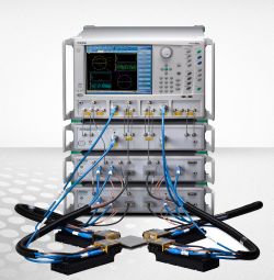
Navneet: The Vector Network Analyzer plays a very critical role in making all the measurements that we have discussed so far, be it in 5G or 6G. A VNAs basic functionality is to input a signal into a device and observe the output signal that comes out from the device after passing through it. A VNA is based on a tuned receiver approach where the receiver port is already aware of what the transmitting port is transmitting in terms of frequencies and power. The work of a VNA becomes even more important in the 6G era, as the devices are going higher and higher in frequencies and smaller and smaller in size. The art of inducing a very accurate and precise signal into the device and then monitoring/detecting the output signal which may be extremely low in power is the most important characteristic of a VNA. A VNA is capable of sweeping a signal from a very low frequency to extremely high frequencies, which means that the 6G devices can be characterized for a very broad frequency range. Anritsu’s VectorStar is the only VNA in the world capable of sweeping from 70 kHz to 220 GHz in a single sweep. There are other applications where the 6G devices are required to be tested only in a banded fashion which means that the user is interested in sweeping only a certain band of operation. VNAs can be combined with external mmWave multipliers to just make banded frequency measurements. Either banded or broadband, the VNA still plays the most important role in any of the device characterization/modelling measurements.
Same is the case with high frequency material measurements. Even for making material measurements, the main engine that drives and calculates the effective permittivity, loss tangents, conductivity etc. is still a VNA. All these parameters are calculated from the base S-parameter measurements done by the vector network analyzer. Even for material measurements, based on the application and expectations from the users, it could either be a banded measurement (mostly) or could be a broadband measurements as well. For material measurements, along with the VNA, a user also needs an appropriate fixture for placing the MUT inside it and then making the measurements.
Since most of the 6G active/passive components and devices are on-wafer and operate at very high frequencies, a VNA combined with a probe station (manual or automatic) and the right pitch probes forms a complete solution for measuring any 6G components/device.
In all, a VNA forms the basic building block for any 5G/6G measurements whether it’s in the design stage, in packaging stage or in the final product stage. Each and every stage requires extensive testing and re-confirmation to verify that the device is successfully working. The VNA guarantees that performance.
6. What solutions does Anritsu offer for 6G measurement and analysis applications?
Navneet: Anritsu offers several solutions for 6G. One of the most important is the vector network analyzer solution that sweeps the broadband frequency range from 70 kHz as the minimum, lower frequency to 110/125/145/220 GHz as the maximum frequency in one single sweep. This has proven to be a big advantage for customers doing device characterization and device modelling. Until recently, measurements were made in a banded fashion (e.g., 90 to 110 GHz, 110 GHz to 140 GHz, and 140 GH to 220 GHz) and later on switching the banded measurements to see the response of their devices over a wide range of frequencies. There were a lot of discontinuities in the measurements with the banded approach and many challenges in buying several banded mmWave modules, waveguide to probe interfaces, and probes. These were needed just to change the entire setup from one band to the other, and along with challenges for repeatability, installation, and stability of the entire system were a huge setback. Anritsu’s broadband solutions provided them with the single broadband frequency coverage from 70 kHz to 145/220 GHz which saved them a lot of time, energy, and money.
There is no such offering available from any other test and measurement company. Anritsu’s VectorStar is also compatible with almost every third-party solution offered for material measurements solutions. The collaboration has been very useful for customers as they have various options available to choose from the industry. Customers can pick and choose from the expert solution providers in the industry, per their requirement of the materials, and Anritsu’s VectorStar is already compatible with the same.
Not only limited to materials and device characterization, Anritsu’s VectorStar is also compatible with almost every antenna measurement solution. Because of its superior performance and upgradability (number of ports/sources/broadband mmWave support), VectorStar is the number one choice amongst our customers performing 6G antenna measurements. Several measurements included, but not limited to, active and passive 6G antennas, AiP (Antenna in Package) etc. can be made with Anritsu VectorStar.
7. What features do they have that make them particularly suitable for 6G research and development?
Navneet: Anritsu’s VectorStar-based broadband solutions are particularly suitable for device characterization, device modelling, material measurements, antenna measurements, and much more. Some of the features that makes Anritsu’s VectorStar based solution suitable for 6G measurements are:
• Superior dynamic range throughout the entire frequency range
• Very small size of our own mmWave modules using state-of-the-art nonlinear transmission line (NLTL) technology, that provides direct connection to the probes and devices, without involving long, extremely lossy, expensive, and error inducing cables in the measurements
• Extremely stable and accurate ALC right at the interface of the mmWave modules
• Extremely good stability and repeatability in the measurements over time/temperature because of the patented technology (NLTL) being used in our mmWave modules
• Extensive and elaborate calibration algorithms for very high frequency measurements ensuring best in the class calibration and residual specifications
• Advances de-embedding techniques and software algorithms that take care of several scenarios in Universal Fixture Extraction (UFX)
• For active device characterization (like amplifiers), very low input powers are available with VectorStar ~-55 dBm/- 60dBm.
• Compatibility with several third-party solution providers for material measurement/antenna measurements, probe stations, mmWave multipliers, and much more.