
- To develop new components and subsystems operating at very high frequencies, it is essential to have accurate models.
- The accuracy of S-parameters over a wide frequency range is a key factor in ensuring the modeling quality of a component.
- The frequency band of vector network analyzers (VNA) is currently limited to 120 GHz. This is not sufficient for some current or next generation technologies.
- This paper presents a new 220 GHz wideband VNA, and explains how such an instrument can simplify and improve wafer-based S-parameter measurements.
By Christian Sattler, Anritsu
Speed and data throughput are key performance indicators for every modern communication system and even with modern, efficient modulation schemes, this will require large frequency bandwidths. However, this is a limited and expensive resources and band plans up to 40 GHz are already overpopulated with wireless services. Moving to higher frequencies such as D-Band (110 GHz to 170 GHz) is a way out of this dilemma, yet at these high frequencies, semiconductor and circuit design becomes more of a challenge. Gone are the days when a design engineer would start their development armed only with some calculations, a piece of paper and a soldering iron. By contrast, today’s circuit development is based on the use of simulation software. Although this can do an excellent job, even at frequencies beyond 100 GHz, designers need exact models of the active and passive devices used in the design. The lack of these models causes unnecessary and costly iterations during the design process.
To achieve good circuit simulation results, using broadband models over a wide frequency range is essential, even if the final device is only used at a narrow bandwidth. It is important to perform the simulation at a much wider range, particularly to evaluate the stability of a design. In addition, out-of-band emissions, including harmonics, also need to be tested for regulatory reasons. The conventional approach would be to concatenate the measurement results from several banded instruments and combine the data. A drawback of this approach is that it will introduce issues such as different uncertainties, drift, and calibration methods for each of the banded measurements. Also, employing different measurement systems is much more time consuming than using a single instrument for all measurements.
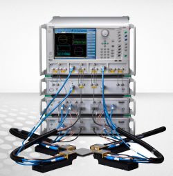
To meet these requirements, Anritsu developed its ME7838G, a 220 GHz broadband VNA. As a technology leader in broadband VNAs, Anritsu can provide a scalable concept for high frequency testing up to several hundreds of GHz. This process started with the introduction of a 110 GHz broadband VNA 10 years ago, followed by the introduction of a 145 GHz system. Now the next hurdle has been passed – 220 GHz in a single sweep VNA. Based on NLTL (Non-Linear Transmission Line) technology, the 220 GHz capability already existed at the Anritsu research center – the biggest challenge was to develop a proper connectivity between the VNA and the device under test (DUT). One route was to develop a completely new coaxial interface, such as a 0.5 mm connector. Standardization of a new connector design is always a very expensive and time-consuming task and since no final device at those frequencies will ever use a coaxial connector as an interface to other components, this option makes little sense.
A broadband interface between the VNA and the on-wafer probe is needed, as the 220 GHz VNA will only be used for the characterization of on-wafer devices. To fulfill the requirement for a broadband response, only a coaxial connector can be used. Yet, as this connector will only be used as an interface between the VNA and probe, a traditional male-female coax connector design with threaded coupling nuts is not essential. The connection must be robust, easy to manufacture and repeatable. Combining a coaxial interface with the robustness and mechanical stability of a waveguide flange is the ideal solution for this challenge. A flanged coaxial connector interface was therefore developed by Anritsu in partnership with MPI to facilitate 70 kHz to 226 GHz continuous swept frequency testing using the ME7838G VNA system.
The Heart of The ME7838G 220 GHz VNA System
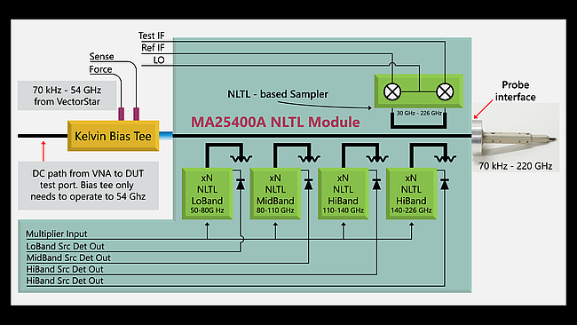
NLTL technology provides excellent conversion efficiency and noise floor performance for optimum system dynamic range at mmWave frequencies. It fits in a small, tightly integrated package for stability and performance. Inside the module, source bands are coupled to the main transmission line through substrate couplers. NLTL harmonic samplers convert test and reference signals to an Intermediate Frequency, from 30 GHz to 226 GHz, and are located as close as possible to the DUT port. An electronic ALC control provides up to 50 dB of power level control. This ALC is important for measurements on isolated transistors and LNAs, which typically require very low drive levels.
Another important attribute is that DC bias can be supplied as usual from the rear connector of the module, removing the need for an extremely broadband bias tee. The main signal path of the module is designed to have very low DC resistance, so a Kelvin bias tee allowing 4-point DC measurements will not introduce noticeable errors.
The RF Interface
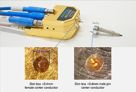
Traditional threaded coax interfaces cannot be scaled down to provide a TE11 mode frequency above 220 GHz. The scaling of standard threaded coupling nut coaxial connectors is not practical for connectors with an outer conductor inside diameter under 0.8 mm. This is because the required machining precision of center conductors and outer conductors simply does not exist. For operation at 220 GHz, a coax interface with a 0.6 mm outer diameter is required, demanding alternative approaches to the design of the connector interface. Also, the possibility to mount relatively heavy waveguide components (used above 110 GHz for calibration and verification purposes) requires a sturdy interface which has an outer conductor that does not flex under load with respect to the connector axis.
A UG-387/UM waveguide interface flange provides alignment for the 0.6 mm coaxial male/female pin connection, thus eliminating the need for a threaded connector. An additional benefit is the mate compatibility with a standard waveguide interface. This can be achieved with an in-line coaxial to waveguide transition. While true waveguide applications are not the normal use cases for such a VNA, the lack of calibration equipment (such as a power meter) still requires such an interface for routine verification procedures above 110 GHz.
Important aspects of such an interface are repeatability and lifetime.
Even after 1000 reconnections, the interface shows negligible electrical degradation.
Device Connectivity
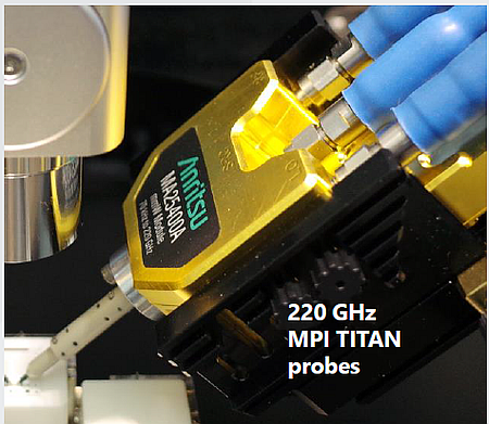
An RF probe provides the link between the coaxial interface of a VNA and the actual DUT placed on a wafer probe. This probe needs a broadband responsivity with low insertion loss and good return loss up to 220 GHz. MPI TITAN™ probes are designed to be used with the Anritsu ME7838G VNA system. They incorporate 50 Ohm MEMS contact tips, they mate directly to the MA25400A modules and provide excellent repeatability and lifetime. The key advantage of this system is a direct connect interface between probe and VNA, ensuring best raw directivity and measurement stability. Also, MPI offers the necessary calibration substrate, supporting the use of modern calibration methods such as LRRM, ALRM and MultiLine TRL.
As well as its large number of built-in calibration methods, the Anritsu ME7838G system is also supported by QAlibria, MPI’s calibration software package. QAlibria simplifies the complete on wafer calibration process and ensures the best possible measurement accuracy.
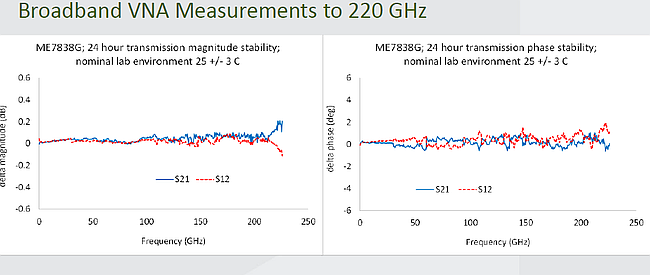
Broadband Measurement Performance
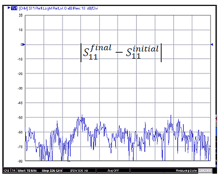
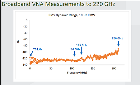
While the ME7838G system is fully specified up to 220 GHz, a picture can say much more than pure numerical data.
Another key aspect for any VNA is drift and the required recalibration interval. The tightly integrated NLTL modules offer excellent stability over time. This is also important since de-embedding, which is needed to move the reference planes from the probe tips to the device, relies on stability.